
Investigating the ET-SoC-1 NoC
Because why ask your RTL engineers when you can have some fun

Investigating the ET-SoC-1 NoC
Ainekko purchased Esperanto’s IP and is developing in the public - the chip was and still is a good idea; we believe that there’s a place for a open computing platform based on said IP, providing beyond what GPUs can offer architecturally. ET-SoC-1 is the beginning. We are taping out our test chip. Until the package from TSMC shows up, ET-SoC-1 is what I’m working on.
That’s my elevator pitch as an engineer working at Nekko.
As Nekko develops in the public: I can share almost everything we do. Ironically this is the best devrel possible. Show, not only tell. I am partially done with basic kernel work in our LLM inference stack and starting to look at the processor as a proper systolic array and see what is possible. Looking at Esperanto’s code. There’s little use of the fact that the processor is a grid of cores. Either Esperanto figured out that it is not worth the effort or they are unable to make use of that fact. I don’t know which. And I care about my performance running FlashAttention and matrix multiplication on llama.cpp. Yet efforts continuously end up with “the bandwidth doesn’t make sense and I am optimizing blind”. To understand what we are working with, this is the rough NoC layout:

And so experiments we do. First, what’s the bandwidth across shires? To be specific, what if we transfer a large-ish chunk (960B, to avoid aliasing in L2) across pairs of shires via TensorLoadL2SCP (think: hardware DMA against other shire’s scratchpad)?

Despite potential shires being yielded for.. yield reasons. The internal logical layout seems to be clean. The bandwidth shows a clear-ish 8x4 pattern in bandwidth. Matching the SoC-1 datasheet’s core layout with shire id incrementing in the y direction. Bandwidth reduces per hop away, but I assume that’s more latency than throughput. And the NoC is symmetric, there is no difference in bandwidth between sending and receiving.

Question: does the shire id map to the physical location? ... We see bands so that has to mean NoC hop. But it is scrambled and not the simple pattern of physical location = shire id. Running simulated annealing we can figure the topology:

The next natural question: How does congestion work on this NoC? Does it work like some chips where each link between nodes can congest? Is the NoC half or full duplex? Does the NoC have directionality?

Measurement results say the NoC is bidirectional and/or the bandwidth is so high that the amount of traffic can be sustained without congestion. I cannot tell if the NoC is sized to match the rest of the chip (maybe.. but questionable choice as that means most usage will underutilize the bandwidth and waste of chip power and area) or the simple pattern is too trivial and Esperanto has designed to solve the specific case. I can’t tell from numerical results. Some further pattern testing shows the same thing:
Scenarios:
disjoint_adj_8: 8 independent flows (0->1, 2->3, 4->5, 6->7, 8->9, 10->11, 12->13, 14->15) on disjoint shire pairs. Does aggregate scale linearly?
disjoint_adj_16: Same but scaled to all 32 shires
parallel_cols_4: 4 long flows (0->16, 1->17, 2->18, 3->19) down parallel columns. How does that work?
row_crossing_4: 4 flows (0->7, 1->6, 2->5, 3->4) in the same row that overlap. Does that congest?
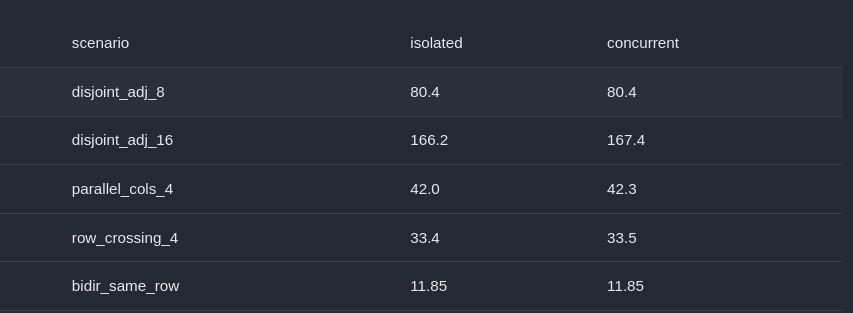
Apparently no. No congestion at all. It seems the only congestion I can find is source read bandwidth. As more and more shires try to read from the same source, bandwidth plateaus. But again I cannot tell if this is a read port limitation or L2 only supporting that read bandwidth. And it’s kinda suspicious that the measured max L2SCP bandwidth is around the claimed DRAM bandwidth on the card. Coincidence? Your guess is as good as mine.

If I target Shire 14 as the source (center of the chip). Aggregate bandwidth from L2SCP to all shires should be higher, right? Also no. It actually achieves a lower peak and aggregate bandwidth drops off at the end. NoC packet congestion......?
")
I am as baffled as you are. New question: How does the DRAM work? Does it follow the same pattern? Let’s just read from the DRAM both in single shire and all shires..

It is surprisingly even. I would expect more performance variance as shires are further and further away from the DRAM. Wherever the DRAM is. But again, the NoC is faster than the DRAM bandwidth (thank god I am not working on a NoC congested chip again). Especially the block diagram in the datasheet tells us nothing about where the DRAM is on the NoC. The best guess I have given the memory read pattern:

Also the Programmer’s reference manual is unclear on how L3 is used. Especially in the context of the TensorLoadL2SCP command.
The TensorLoadL2Scp instruction copies a tensor from memory, bypassing the L1 data cache and the L2 cache, to the L2 scratchpad.
Doing some benchmarking.. we can see that performance drops if the reading set is larger than ~32MB. Which coincides with the default L3 configuration (1MB per shire, 32MB total).

Given we kinda know where the Memshire lives and can observe its effect on bandwidth, and we have a problem getting the full 120GB/s during real workload. Can we do the same trick as some other grid-like AI accelerator companies and make shires send requests to one specific Memshire? So we can maximize memory access pattern and avoid crosstalk...
Not at large intervals, which is expected because that’d be a terrible design

We can find patterns at really small intervals -- at near the cacheline size, we find a pattern of 512B.. so 8 cachelines (cacheline size is 64B).. mapping to the 8 Memshires?

Which if we fold the cacheline sized graph along 8 cachelines. We get the following diagram. That clearly shows different bandwidth to different Memshires, up to 50% difference.

With that knowledge we can hit the specific lines that we know the access goes to specific memshires, loading from a different address to avoid L3 effects. And bingo! We found approximately where each memshire is and the achievable bandwidth from them with only one shire asking for data:

Now the final and obvious question - where does the memshire live on the NoC? ... but before that the other question - is the 8x4 mesh correct? We assume the underlying is 8x4 because that’s what the datasheet and PRM say. We all know these can lie. Let’s do the same simulated annealing but make the topology itself also part of the model. And see if we can predict the bandwidth:

So documents do lie. Turns out it is a mesh... but with missing links (I assume yield reasons, so the topology on your chip might differ), definitely not the 8x4 mesh that you’re lead to believe according to the datasheet product brochure and we can almost perfectly express the bandwidth between shires as a function of hops given the right topology. But that hole at 5,3 feels suspicious. And there’s outliers in the predicted bandwidth. Why does our standard deviation suddenly go from very small to 0.25? Unless... there’s other nodes that exist on the NoC that passes through NoC transparent from/to the shires, but it itself not a compute shire so I cannot measure the bandwidth of it. What if I just add a node there? Does that improve my predictive power?
 as a unknown NoC router")
And now all the outliers are gone. That left me suspecting the 3 empty nodes are actually also routers. Maybe...? But there is not enough topological information to determine their existance or not. By the same approach we can figure out where the memshires lives on the NoC -- the predictive power of the graph is already high, so they must not sit on their own NoC hop in the mest, either outside of the current mesh or they inject themslves into the mesh. Some simulated annealing later... We have the result. Note that I (personally) assumed the injection location is not uniform. Memshire 0, 1 and 7 have 2 locations (because the plots seem to indicate so). But know this is likely wrong and contaminated by L3 access speed as chip floorplan would be insane if designed as so:

And we can update our visualization of Memshire access performance and it looks absolutely beautiful. But this does not sit well with me - you wouldn’t put memory access at the center of the NoC. Maybe it’s L3 working as intended? Instead of shrire -> Victim L3 -> shire (not found) -> memshire it chip dpes shrire -> Victim L3 -> memshire -> shire? Either way bandwidth is bandwidth and that’s what matters for a real kernel.
")
We can finally figure out the max bandwidth possible against a single memshire. And calculate the actual peak bandwidth achievable to be ~88GB/s on my specific chip.

As a side note. I tried to figure out if I can use latency instead of bandwidth to locate the Memshire. No. Atomics share the same pattern. Presumably the chip uses L3 as the atomic target instead of DRAM. Fair. But apparently atoics have a baseline 120 cycle latency regardless of where they are in memory (plus measurable overhead, but that’s relatively low). And each hop contributes a clean 6 cycle latency increase. Which indicates 3 cycles per direction.

The ET-SoC-1 chip is really nice. It behaves like a flat processor without the NoC being super obvious. You can still see it. And you can still use it. But most applications ought to treat the processor as a flat array of cores and not step onto any footguns. Best of both worlds.