
The Next Thousand Chips
aka AInekko's Manifesto

Most emerging semiconductor startups are trying to be the Nvidia-killer. That means two- to three-year design cycles, chasing the newest and most expensive process nodes, big teams that barely fit in a group photo on the website, billions of VC dollars.
This framing is already outdated.
It assumes that the problem is to outperform existing architectures under the same design constraints: similar toolchains, similar abstractions, similar iteration cycles. It assumes the bottleneck is architecture, ISA or pure execution.
The old chip design stack was built around human scarcity and walled gardens. RTL, compilers, EDA flows, licensed IP, NDAs, verification boundaries, and organizational handoffs all made sense when the central problem was helping humans divide a system too complex to hold in one’s mind.
Even with AI agents applied to chip design everybody rushed to make the old stack faster, write verification faster, help with synthesis. All these efforts are empowering the same teams with the new tools, but at the end of the day Conway’s law still means you “ship the [old] org chart”. Same happened with SW at first with co-pilots that were effectively autocomplete on steroids, before agentic systems entered the scene.
The next frontier will be defined by how many architectures can be explored, tested, refactored, and specialized by small teams using AI as a true collaborator. But how to open the chip design space to more people than just a handful of well-funded chip designers? What is missing?
The answer is not a better RTL generator.
Agents change the search space
Agents do not need to respect the boundaries humans created between software and hardware, they don’t need PyTorch, CUDA, PTX or similar abstraction layers.
If you can vibe-code directly in assembly, you don’t need a compiler.
If you can reliably vibe-code RTL, you don’t need the layers above it.
If the design process itself becomes programmable, even RTL starts to look like an unnecessary intermediate representation. We are not suggesting vibe coding GDS just yet, but you get the idea.
Should you be asking AI to create chip design from scratch? Not really – it is an infinite search space. What agents can do is reason about model structure, data movement, memory layout, compute topology, scheduling, microarchitecture, and RTL as coupled choices. This turns hardware design into an end-to-end optimization problem: given a workload and constraints - find the best implementation across the software-hardware boundary. It’s still the human’s job to choose the constraints and the optimization function, otherwise the search will not converge, and you’ll get a hallucinated result.
Collapsing the stack
Intent, optimization function and constraints – how do we start?
Luckily, we are not the first ones to start asking these questions.
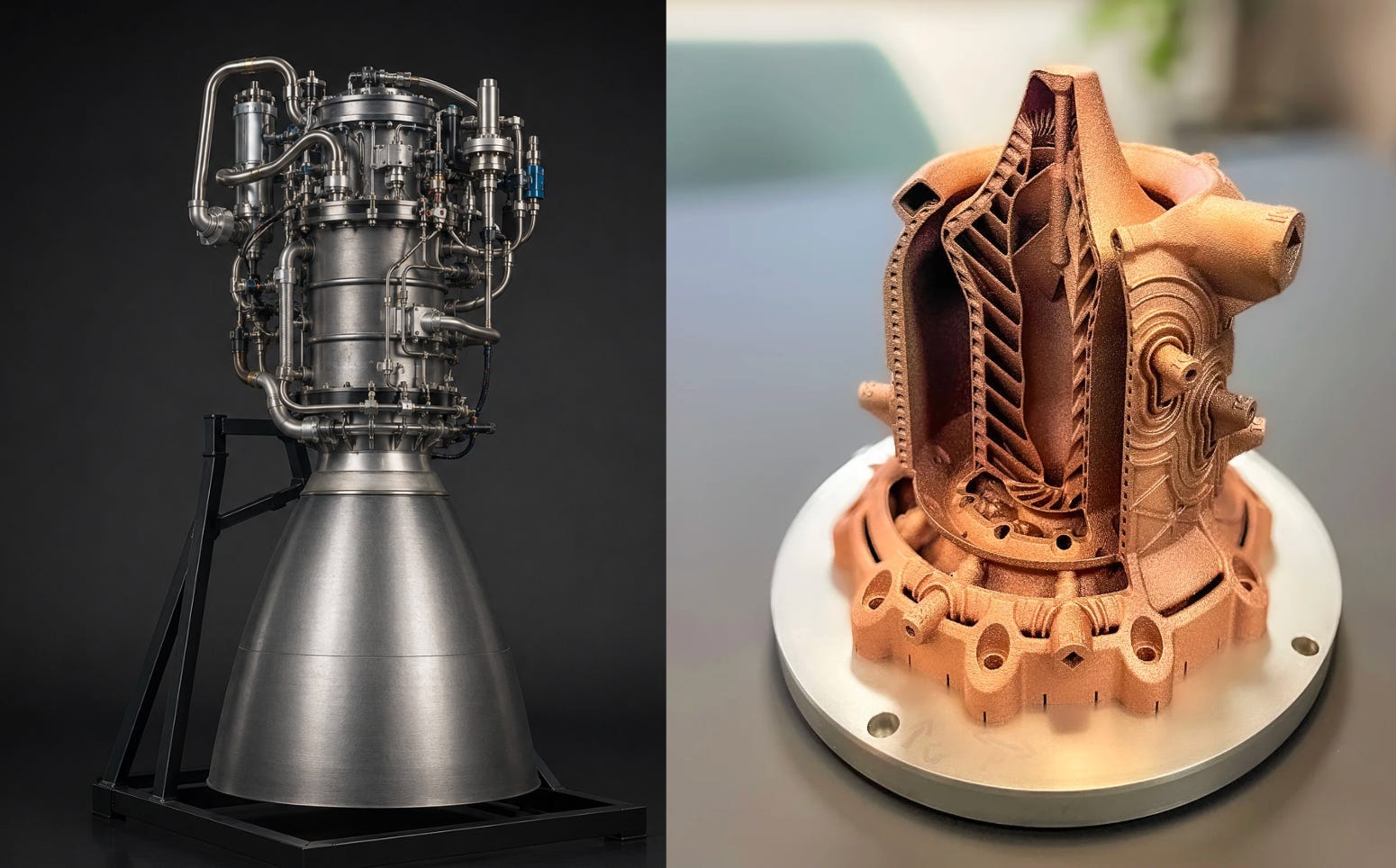
One approach that works well is narrowing the goal. And the most prized goal right now is running AI models at the top speed ASICs are capable of. Models are defined by compute graphs and those are not Turing complete programs. If you fix the model, you can take the model graph and lower it directly into hardware implementations, bypassing traditional layers – etch the model into the chip. That’s what Taalas did compiling models directly into Verilog, showing 50x improvement vs Nvidia.
This approach took away the notion that abstraction stack is sacred.
But it only makes sense economically if that one model you lower is extremely popular and that constitutes a big market segment. For fast evolving markets or proprietary models, it doesn’t work that well.
If you want some level of reusability of your ASIC, the constraint space is not as tightly defined, so you need to introduce some other guardrails to make the search reasonable. E.g. give agents a structure, or a substrate to map models to. And in an interesting experiment in the University of Toronto (Talos V2), team of researchers and agents started with transformer model structure not a single model and ended up discovering a need for a substrate to map it to - some kind of reusable tile. Spoiler alert: they chose systolic arrays. More flexible yet not an architecture from scratch.
With the explosion of Physical AI use cases, the requirements for the diverse collection of chips are back in the game, too – it’s not just one homogeneous data center environment we are talking about – size, power, latency and other constraints, but new models and model architectures create pressure that old school chip vendors can’t sustain.
Now another question, what if we can give agents a real flexible substrate that can be morphed into many things?
Open Substrate
The substrate has to be real. It must come from hardware that has survived contact with implementation and usage, not just from academic exercises that have never been taped out.
The substrate has to be open. No IP licenses, no NDAs, no worries about foundational LLMs CLAs - agents are welcomed.
The substrate has to have tests, simulation, co-simulation, synthesis paths, examples, documentation, and clear contribution flows.
Luckily now there is a substrate like that.
And it lives under the name CORE-ET in the OpenHW Group of the Eclipse Foundation.
CORE-ET is not a white paper about future chip design. The Erbium branch is the exact design that we have taped out and expect back from TSMC in a few months. It’s also a piece of a bigger design that has been taped out 5 years ago and still stands as a useful and very energy efficient chip sporting 1088 minion cores.
How sophisticated are the Minion cores? Here comes the geeky part. Minion is a tightly optimized, dual-threaded RISC-V core: small enough to replicate aggressively, predictable enough to compose into larger fabrics, and flexible enough to sit at the center of many different architectures. It has an optional vector/graphics coprocessor for dense data-parallel work.
But the real unit of design is not the core. Eight Minions are packaged together into an atomic compute tile: efficient, coordinated, and shaped for systolic-array-like fabrics. If you want a hint about the design philosophy, remember that the T in ET stands for Transputer.
That is what makes CORE-ET interesting as substrate. It is a reusable unit of compute: compact enough for experimentation, powerful enough to matter, and structured enough for agents to reason about.
The gory microarchitectural details are here.
But! It’s not just RTL, it comes with real chips, programmer’s manual, simulator, runtime, optimized kernels, even a bare metal Go implementation. It can exist in the old school paradigm. 1 tile delivering roughly 1 TOPS at 0.5W.
But for us this RTL is not the final product. It is the source material. It contains real implementation knowledge: the decisions, scars, constraints, and structures that only exist when a design has been pushed toward silicon.
And the things that we were able to do with it (with the help of agents) are the beginning of a bright future where the chip design gets unlocked for millions of developers.
New Economics
Once design is grounded in a composable substrate, the entire cost structure shifts.
Iteration becomes cheap.
Exploration becomes parallelizable.
Specialization becomes viable at a much smaller scale.
The limiting factor is no longer the cost of committing to a design, but the ability to search through possibilities efficiently.
Even better the composability finally gives a boost to chiplet design. Tape out building blocks. Recompose them for different use cases. Increase the agentic search space to multiple composed blocks. Get custom chips without custom tape outs.
The difference is not incremental. It is structural
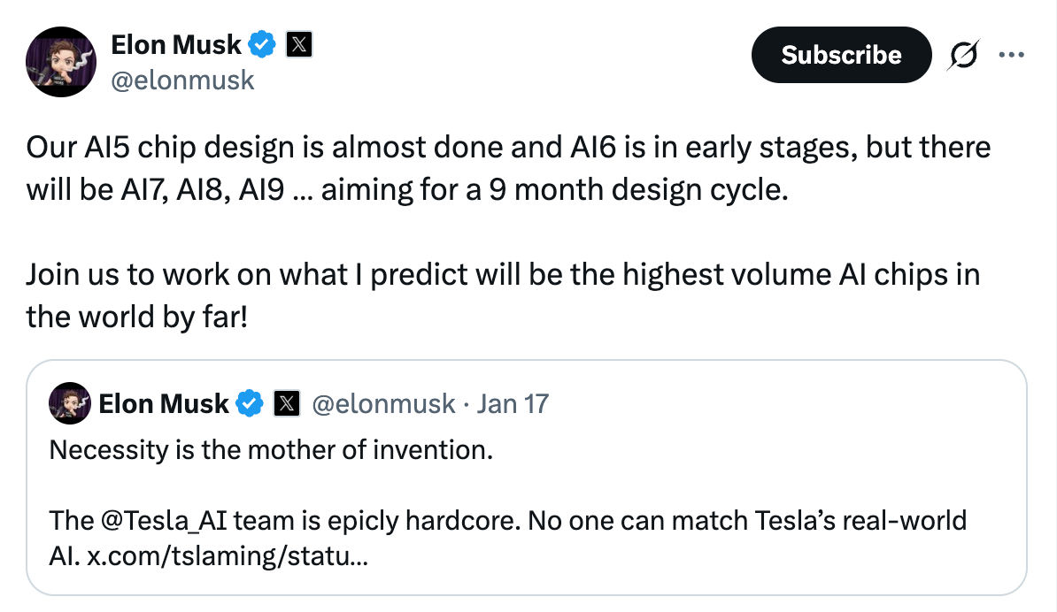
It’s the difference that can serve the demand of a tape out every 9 months even if you are not Tesla.
What’s next
CORE-ET is not the only thing we have. We have a treasure trove of IP developed over the course of 10 years by a talented team of engineers in the old paradigm. Like any other chip company on the mission to fight Nvidia they have developed a lot of things (even the RBOX!), and we aim to keep open sourcing them with the same purpose of getting more substrate for agents.
Luckily the substrate is so flexible that with agentic help you can turn it almost into anything – from systolic array architecture to Turing complete coherent blocks, from 8 core to 4000+ cores, we even have big out-of-order cores that are not so easy for agents to design right now but maybe with the right substrate?
We also are open source people, so we couldn’t shy away from open tools. And guess what? With small enough designs you not only can put them in FPGAs by tool calling Yosys in the matter of hours, but you give the open source SkyWater PDK to the agents and go through place and route with OpenROAD and you get yourself a Tiny Tapeout. Not just one chip-per-student anymore – one chip per Claude session!
Memory is next. It’s already emerging as the next bottleneck as both Taalas and Talos discovered. How to store the weights throughout the system, how they move, how they are reused, and whether they should move at all is defining the next phase of substrate design.
That deserves its own post.
For now, the point is simple: the old race was to build one giant architecture to serve them all.
The new race is to make the next thousand chips.